Please contact us at:+86-755-23600835
Nondestructive testing encompasses an array of examination approaches with a proven record of not adversely affecting a component's performance or dependability.These techniques serve to detect markings, voids, and other irregularities within or on components.
X-ray images are compared against OEM parts and are also used to verify that no voids have formed and to confirm leads and bond wires.
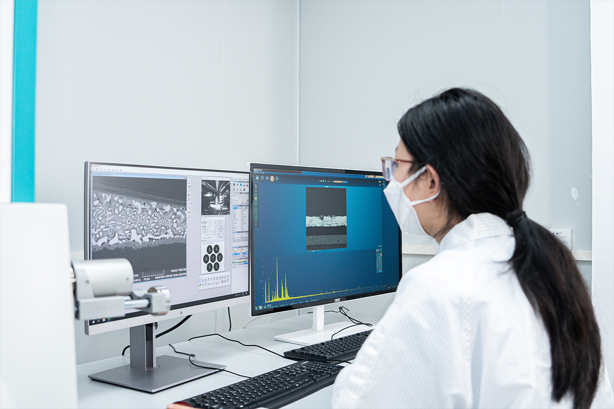
Analyze the chemical elements and their content of metal or inorganic non-metallic materials.
C-SAM acoustic microscopy reveals internal structures and defects in electronic components through sound wave imaging, providing crucial insights into surface-invisible issues, ensuring product quality and performance align with standards.
The role of a Curve Tracer in electronic components is to identify defects and faults by graphically displaying electrical characteristics, ensuring proper functionality, and conducting quality assessments.
Destructive testing represents the final stage in R&A's procedure for confirming legitimacy. In certain cases, more invasive techniques, such as decapsulation and lead solderability testing, could be necessary to validate the authenticity of a product.
Decapsulation serves to validate the dimensions of the die, examine the branding of manufacturers, assess the internal structure of the die, and verify component identification numbers in electronic devices.
Heated-solvent testing identifies counterfeiting indications through the identification of sand marks, variances in texture, and the presence of blacktopping.
R&A assesses the solderability of component leads to assess the durability of coatings and examines aged products for indications of corrosion and oxidation to assess their usability.
R&A evaluates bond strengths and distributions, as well as assesses the integrity of materials utilized for attaching dies or surface-mounted passive elements to ensure they meet bond-strength requirements.


In addition to the above standards, WG can provide other anti-counterfeiting tests according to specific customer requirements.
Contact us to learn more about our anti-counterfeiting testing services.